The mainstream tech press is currently swooning over reports from Beijing. The China National Nuclear Corporation just announced it has achieved mass production of highly enriched silicon-28 with a purity level exceeding 99.99 percent. The lazy consensus among commentators is that this development solves the supply bottleneck for quantum chips, offering a shortcut to scalable quantum computation while bypassing Western trade restrictions.
They are celebrating a structural dead end.
I have spent over a decade assessing advanced hardware supply chains and hardware development cycles. I have watched organizations torch hundreds of millions of dollars chasing high-purity material breakthroughs, only to discover that material purity cannot overcome fundamental architectural flaws. The current applause for industrial-scale silicon-28 enrichment misses the actual engineering reality of quantum information processing. This is not a geopolitical checkmate. It is a highly expensive solution to the wrong problem.
The Spin-Free Fallacy
The technical justification for enriching silicon-28 sounds pristine on paper. Natural silicon is composed of three isotopes: silicon-28, silicon-29, and silicon-30. Silicon-29 makes up about 4.7 percent of natural silicon and possesses a nuclear spin of one-half. This nuclear spin acts as a microscopic magnetic disturbance. For a spin qubit embedded in a silicon crystal, the fluctuating magnetic fields of nearby silicon-29 atoms act as chronic environmental noise. It randomizes the qubit state, causing rapid decoherence—the loss of quantum information.
By removing silicon-29 and achieving 99.99 percent pure silicon-28, you create what physicists call a "semiconductor vacuum." Because silicon-28 has zero nuclear spin, the magnetic noise vanishes. Qubit coherence times shoot up dramatically.
This is where the mainstream narrative stops thinking. They assume that longer coherence times automatically mean scalable quantum computers. They fail to look at the severe spatial constraints of the silicon architecture itself.
The Two-Nanometer Trap
To perform quantum logic operations, qubits must interact with their immediate neighbors. In a silicon spin architecture, this interaction relies on exchange coupling—the overlap of electron wavefunctions between adjacent quantum dots.
The physical mechanics of wavefunction overlap dictate that the distance between these quantum dots must be incredibly small, typically between 10 and 15 nanometers. This is not a macro-scale manufacturing problem; it is an atomic-scale alignment problem.
Imagine a scenario where you have to position thousands of individual electrons with nanometer-level precision, then route control lines—gates, ohmic contacts, and readout lines—to every single one of them. The sheer density of electrical wiring required to control a million-qubit silicon chip creates an immediate physical impossibility.
You cannot route lines that are smaller than the atoms they are made of. When you pack control lines that closely, you introduce severe capacitive crosstalk. The control signals intended for qubit A inevitably bleed into qubit B, completely destroying the fidelity of your logic gates.
Mass-producing ultra-pure silicon-28 does absolutely nothing to solve this spatial routing crisis. You have merely created a quieter graveyard for your qubits.
The False Promise of CMOS Compatibility
The second pillar of the silicon quantum hype is the claim that it can leverage existing commercial semiconductor manufacturing lines. Proponents argue that because the global tech industry already knows how to manufacture billions of silicon transistors, transitioning to silicon quantum chips will be straightforward.
This argument conflates basic material compatibility with process compatibility. Commercial fabrication facilities are optimized for classical transistors that operate via the collective movement of millions of electrons at room temperature. Quantum dots require the absolute isolation and manipulation of single electrons at temperatures below 100 millikelvin—just a fraction of a degree above absolute zero.
The defects that commercial foundries consider acceptable—microscopic charge traps at the interface between the silicon and the insulating silicon dioxide layer—are fatal to a quantum dot. A single trapped charge near a quantum dot alters the local electrostatic environment, shifting the operating voltages and rendering the qubit useless.
Achieving 99.99 percent isotopic purity in your bulk silicon material does not fix the disordered atomic mess at the oxide interface where the qubit actually lives.
The Cross-Disciplinary Delusion
Why is the industry blind to this? Because the field suffers from deep structural silos.
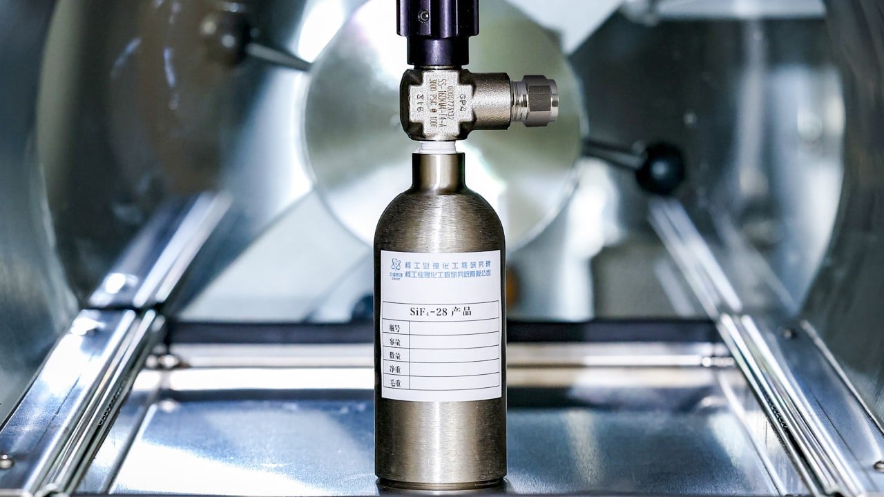
The nuclear physicists and material scientists who developed the centrifuge separation techniques at the Research Institute of Physical and Chemical Engineering of Nuclear Industry in Tianjin are focused entirely on isotopic yield. They measure success by the decimal points of abundance.
The quantum physicists writing papers on single-qubit coherence times measure success by how long a single isolated electron can hold its spin state in a dilution refrigerator.
Neither group is responsible for building a functioning, multi-layer, million-qubit routing architecture. When you talk to the lithography engineers who actually have to print these designs, the mood changes instantly. They will tell you that the defect tolerances required to make exchange-coupled quantum dots uniform across a large wafer do not exist on any manufacturing floor, anywhere in the world.
Where the Real Battle Is Being Fought
While Beijing pours capital into isotopic enrichment plants to secure raw materials, alternative computing paths are quietly undermining the necessity of silicon entirely.
Neutral-atom quantum systems, for example, do not use solid-state chips at all. They trap individual atoms in optical tweezers inside a vacuum chamber. Because the atoms are suspended in empty space, they do not suffer from the material defects, interfacial charge traps, or manufacturing non-uniformities that plague silicon. More importantly, neutral atoms can be moved physically using lasers, allowing dynamic reconfiguration of qubit connectivity during a calculation.
Superconducting circuits, despite their massive physical footprint, use lithography features that are orders of magnitude larger than silicon quantum dots. This makes them significantly easier to fabricate uniformly using existing techniques.
Silicon-28 is a luxury material for an architecture that is fundamentally restricted by the laws of electrostatic routing and interface physics. Having a massive domestic supply of pure silicon-28 is useful if you are building high-end navigation gyroscopes or advanced metrology standards. But as a foundation for scalable quantum computing, it is an incredibly precise key for a lock that has already been welded shut.
The real metric of progress in the quantum sector is not material volume; it is gate fidelity under scalable wiring conditions. Until someone demonstrates a multi-thousand qubit silicon architecture that can handle its own control wiring without overheating or leaking signals into adjacent nodes, mass production of raw isotopes is just an expensive exercise in sorting atomic beans.
Stop measuring quantum readiness by the purity of the substrate. Start measuring it by the reality of the interconnects.